INTEGRATED CIRCUITS DIVISION
MX884
R01
www.ixysic.com
3
1 Specifications
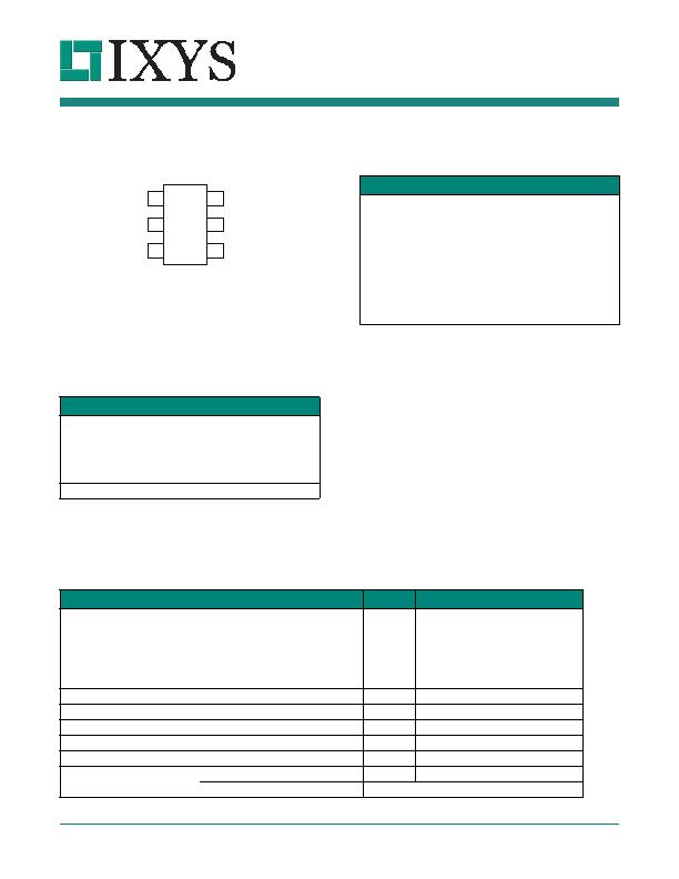
1.1 Package Pinout
1.2 Pin Description
1.3 Absolute Maximum Ratings
Absolute maximum electrical ratings are at 25癈
Absolute maximum ratings are stress ratings. Stresses in
excess of these ratings can cause permanent damage to
the device. Functional operation of the device at conditions
beyond those indicated in the operational sections of this
data sheet is not implied.
1.4 DC Electrical Characteristics
V
IN
=5V, T
A
=25癈.
6
5
4
Pin#
Name
Description
1
SCK
Serial Clock
2
GND
Ground
3
LOAD
Load-Side Connection to the
External Sense Resistor
4
IN
Positive Supply Terminal and Power
Connection for the External Sense
Resistor
5
CS
Chip Select (Active Low)
6
SDO
Serial Data Output (Open Drain)
Parameter
Symbol
Min
Max
Units
IN Supply Voltage
-
-
70
V
LOAD
-
-
70
V
SCK, CS Input Voltage
-
-
6
V
SDO Open Drain Pull-Up Voltage
-
-
6
V
Operating Temperature Range
T
A
-40
+85
癈
Storage Temperature Range
T
STG
-55
+150
癈
Parameter
Conditions
Minimum
Typical
Maximum
Units
Operating Voltage Range (V
IN
)
-
3
-
60
V
Supply Current
I
LOAD
=0
-
0.25
-
mA
Average A/D Reading
10mV Sense Voltage
90
100
110
LSB
Average A/D Reading
100mV Sense Voltage
992
1000
1008
LSB
Output Noise
C
S
=10nF Parallel, R
S
=10W
-
1.5
-
RMS LSB
SCK Pulse Period
-
5
-
-
ms
SCK Pulse Width
High or Low
200
-
-
ns
CS Pulse Period
-
100
-
-
ms
CS Falling to First SCK Rising
-
200
-
-
ns
Last SCK Falling to CS Rising
-
100
-
-
ns
SCK Falling to SDO Valid
SDO Falling
-
-
80
ns
SDO Rising
Depends on SDO R, C
-
发布紧急采购,3分钟左右您将得到回复。
相关PDF资料
NCP1080DEG
IC CONV CTLR POE-PD 13W 20-TSSOP
NCP1081DEG
IC CONV CTLR POE-PD 40W 20-TSSOP
NCP1082DEG
IC CONV CTLR POE-PD 13W 20-TSSOP
NCP1083DEG
IC CONV CTLR POE-PD 40W 20-TSSOP
NCP1501DMR2G
IC REG SGL BUCK/LINEAR 8MICRO
NCP1578MNR2G
IC REG DL BCK/LINEAR SYNC 20-QFN
NCP1601BDR2G
IC PFC CTRL CRM/TRANSITION 8SOIC
NCP1603D100R2G
IC CTLR PFC/PWM COMBO 16-SOIC
相关代理商/技术参数
MX8870
制造商:未知厂家 制造商全称:未知厂家 功能描述:Controller Miscellaneous - Datasheet Reference
MX887D
制造商:CLARE 制造商全称:Clare, Inc. 功能描述:μPower Hall-Effect Switch
MX887DHT
制造商:IXYS Integrated Circuits Division 功能描述:MX Series 5.5 V 2 mA Surface Mount Power Hall-Effect Switch - TSOT-23-3
MX887DHTTR
功能描述:板机接口霍耳效应/磁性传感器 Power Hall Effect Switch w/Open Drain Output 3-lead TSOT-23 on T&R RoHS:否 制造商:Honeywell 类型:Bipolar Hall-Effect Digital Position Sensor 工作电源电压:3 V to 24 V 电源电流:3.5 mA 最大输出电流:20 mA 工作点最小值/最大值:5 G, 55 G 最小/最大释放点(Brp):- 55 G, - 5 G 最大工作温度:+ 150 C 安装风格:SMD/SMT 封装 / 箱体:SOT-23
MX887P
制造商:CLARE 制造商全称:Clare, Inc. 功能描述:??Power Hall-Effect Switch
MX887PHTTR
功能描述:板机接口霍耳效应/磁性传感器 Power Hall Effect Switch w/Push-Pull Output 3-lead TSOT-23 on T&R RoHS:否 制造商:Honeywell 类型:Bipolar Hall-Effect Digital Position Sensor 工作电源电压:3 V to 24 V 电源电流:3.5 mA 最大输出电流:20 mA 工作点最小值/最大值:5 G, 55 G 最小/最大释放点(Brp):- 55 G, - 5 G 最大工作温度:+ 150 C 安装风格:SMD/SMT 封装 / 箱体:SOT-23
MX88L284AEC
制造商:未知厂家 制造商全称:未知厂家 功能描述:Highly integration chip for Flat Panel Display application
MX88L285-S
制造商:未知厂家 制造商全称:未知厂家 功能描述:Converter